
EUV-IUCC
EUV lithography is
a state-of-the-art lithography technology that has finally begun to be applied to 7nm node semiconductor high volume manufacturing in 2019, only 38 years from the beginning of research in 1981.
IUCC
The acronym "IUCC" stands for ‘Industry-University Collaboration Center’, which means working together on a common goal. Through cooperation, the industrial and academic members within the center develop an enhanced view of how to achieve their objectives. We combine our leadership in EUV technology with in-depth expertise to form the foundation of better manufacturing solutions.
We are the sole EUV technology network hub in Korea dedicated to aid sponsoring industries through fundamental and applied research and transfer research results.
-
01
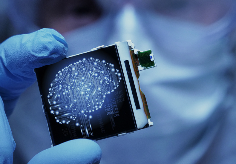
EUV lithography
EUV Lithography is a topnotch technology that implements a sub 7 nm node ultrafine semiconductor device circuit using EUV light with a wavelength of 13.5 nm. EUV is easily absorbed by most materials including the atmosphere, so that all optical systems are reflective, unlike conventional exposure technologies using transmissive optics. In this background, all element technologies need be developed in a completely different way from traditional exposure techniques.
-
02
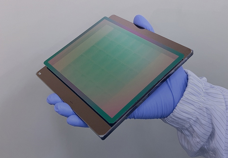
EUV photomask
In optical lithography, a circuit pattern is implemented by projecting a design circuit engraved on a photomask onto a wafer using light. Unlike conventional lithography technology, EUV mask is manufactured with reflective structure but this causes a fatal problem called mask 3D effect. In order to prevent the deterioration of imaging characteristics from mask 3D effect, EUV mask research and development of new materials and structures are actively underway.
-
03
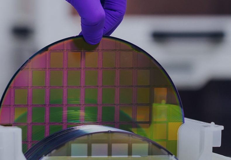
EUV pellicle
As the resolution is gradually improved, wafer pattern loss can also be caused by nanometer-sized contaminants. Although EUV pellicles have been proposed to protect the EUV mask from external contaminants generated during the process to prevent yield degradation, they do not meet the requirements due to extremely difficult technical issues. EUV pellicle research and development with excellent optical, thermal and mechanical properties is being actively performed for this commercially unavailable core element technology.
-
04
EUV resist
Photoresist(PR), which plays a key role in wafer pattern transfer, is directly related to the performance and productivity of the entire lithography process. Resolution, line-edge-roughness and sensitivity are the main characteristics required for the photoresist, but EUV resist development should consider additional issue to alleviate stochastic effects
EUV-IUCC News
-
Data Room
IRDS 2020 Fall
-
 Data Room
2020 Intel Architecture Day presentation files
-
Data Room
2020 EUVL-IUCC June Workshop proceedings
-
Data Room
2020 EUVL-IUCC April Webinar ppt slides 2/2
-
Data Room
2020 EUVL-IUCC April Webinar presentation materials 1/2
-
Data Room
[Open to all] 2019 EUVL Workshop proceeding file
-
Data Room
[Open to all] 2018 EUVL Workshop proceeding file
-
Data Room
[Open to all] 2017 EUVL Workshop proceeding file
-
Data Room
[Open to all] 2016 EUVL Workshop proceeding file
-
Data Room
[Open to all] 2015 EUVL Workshop proceeding file
-
 Data Room
2020 SPIE Advanced lithography proceedings : 7. Progress in EUV Sources
-
 Data Room
2020 SPIE Advanced lithography proceedings : 5. EUV Scanner Monitoring
Send us your request
- [04763] Hanyang University FTC 615, 222, Wangsimni-ro, Seongdong-gu, Seoul, Republic of Korea Tel: +82-02-2220-4407
- Copyright(c) Hanyang Univ Industry-University cooperation Foundation. All rights Reserved.Design By Threeway